|
Navigation
 This wiki
This page This wiki
This page
|
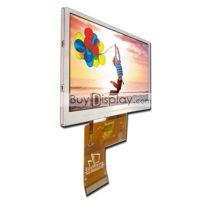
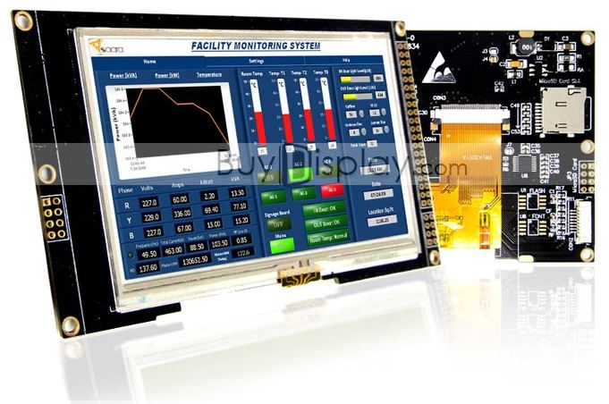
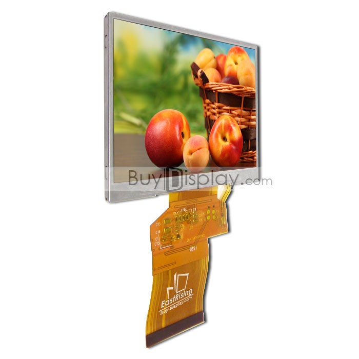
Hardware Design Extension boardsA specific extension board is developed to have nice laboratories for the students. Current schematic of the board. Connectors & i2c addressesLCD+VGA with different sizes supportedER-TFT043-3-3023-2469
ER-TFTM043-4-2781-8080-2765-3.3V-3023-2559-4296
ER-TFT035-3-2034-3275-3127
TX06
TX07-D09VM1CAB
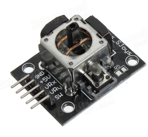
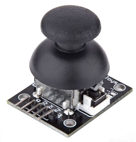
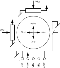
JoystickA joystick as we can found PS-2 extension for players is provided near the LCD. With X & Y analog movement it could be use for games on the display or to control the Pan Tilt system with camera. The connector is 5 pins, +5V powered.
R between Vcc and Gnd = 4 k The resistors are 10k. The idle position is Vcc/2.
The 2 analog outputs are connected to an ADC with SPI connection to the FPGA: MCP3204T The ADC has 4 input, 2 Joystick modules are connected to one ADC chip.
The ADC converter is connected through the SPI interface.
|
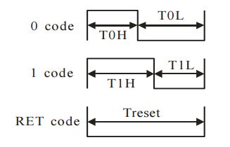
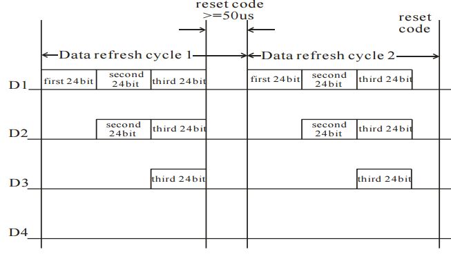
| Timing Name | Time | Tolerance |
|---|---|---|
| T0H | 0.4 us | +/- 150 ns |
| T0L | 0.85 us | +/- 150 ns |
| T1H | 0.8 us | +/- 150 ns |
| T1L | 0.45 us | +/- 150 ns |
| TReset | > 50us |
IR-sensor
OneWire unique ID chip
GPIO Extension connectors
- 40 pins
- 2 rows
- 2.54mm pitch
40 pins connector GPIO 0(J2) Top View
| Name | GPIO_0 | pin | pin | GPIO_0 | Name | ||
|---|---|---|---|---|---|---|---|
| nI2C_Int | GPIO_0_b0 | 1 | 2 | GPIO_0_b1 | PIROut | PIR | |
| Cam_PAL_VGA_SDA | GPIO_0_b2 | 3 | 4 | GPIO_0_b3 | Cam_PAL_VGA_SCL | i2c | |
| PAL_VD_HSO | GPIO_0_b4 | 5 | 6 | GPIO_0_b5 | PAL_VD_VSO | ||
| PAL_VD7 | GPIO_0_b6 | 7 | 8 | GPIO_0_b7 | PAL_VD6 | ||
| PAL_VD5 | GPIO_0_b8 | 9 | 10 | GPIO_0_b9 | Board_ID | OneWire | |
| +5V | 11 | 12 | Gnd | ||||
| PAL_VD3 | GPIO_0_b10 | 13 | 14 | GPIO_0_b11 | PAL_VD4 | ||
| PAL_VD1 | GPIO_0_b12 | 15 | 16 | GPIO_0_b13 | PAL_VD2 | ||
| PAL_VD_CLKO | GPIO_0_b14 | 17 | 18 | GPIO_0_b15 | PAL_VD0 | ||
| Servo0 | GPIO_0_b16 | 19 | 20 | GPIO_0_b17 | Cam_PixClk | ||
| Servo1 | GPIO_0_b18 | 21 | 22 | GPIO_0_b19 | Cam_LV | ||
| From_ESP_TxD | GPIO_0_b20 | 23 | 24 | GPIO_0_b21 | Cam_FV | ||
| To_ESP_RxD | GPIO_0_b22 | 25 | 26 | GPIO_0_b23 | Cam_SysClk | ||
| SPI_MISO | GPIO_0_b24 | 27 | 28 | GPIO_0_b25 | SPI_Ena_n | ||
| +3.3V | 29 | 30 | Gnd | ||||
| J0_SPI_CS_n | GPIO_0_b26 | 31 | 32 | GPIO_0_b27 | SPI_Clk | ||
| J0_SPI_MOSI | GPIO_0_b28 | 33 | 34 | GPIO_0_b29 | SPI_MOSI | ||
| J0_SPI_MISO | GPIO_0_b30 | 35 | 36 | GPIO_0_b31 | SPI_DAT | ||
| J0_SPI_CLK | GPIO_0_b32 | 37 | 38 | GPIO_0_b33 | PIO_SCL | ||
| LED_BGR | GPIO_0_b34 | 39 | 40 | GPIO_0_b35 | PIO_SDA |
40 pins connector GPIO 1(J1) Top View
| Name | GPIO_1 | pin | pin | GPIO_1 | Name | ||
|---|---|---|---|---|---|---|---|
| Video_R0 | GPIO_1_35 | 40 | 39 | GPIO_1_b34 | Video_R1 | ||
| Video_R2 | GPIO_1_33 | 38 | 37 | GPIO_1_b32 | Video_R3 | ||
| Video_R4 | GPIO_1_31 | 36 | 35 | GPIO_1_b30 | Video_R5 | ||
| Video_R6 | GPIO_1_29 | 34 | 33 | GPIO_1_b28 | Video_R7 | ||
| Video_G0 | GPIO_1_27 | 32 | 31 | GPIO_1_b26 | Video_G1 | ||
| +5V | 30 | 29 | Gnd | ||||
| Video_G2 | GPIO_1_b25 | 28 | 27 | GPIO_1_b24 | Video_G3 | ||
| Video_G4 | GPIO_1_b23 | 26 | 25 | GPIO_1_b22 | Video_G5 | ||
| Video_G6 | GPIO_1_b21 | 24 | 23 | GPIO_1_b20 | Video_G7 | ||
| Video_B0 | GPIO_1_b19 | 22 | 21 | GPIO_1_b18 | Video_B1 | ||
| Video_B2 | GPIO_1_b17 | 20 | 19 | GPIO_1_b16 | Video_B3 | ||
| Video_B4 | GPIO_1_b15 | 18 | 17 | GPIO_1_b14 | Video_B5 | ||
| Video_B6 | GPIO_1_b13 | 16 | 15 | GPIO_1_b12 | Video_B7 | ||
| Video_Clk | GPIO_1_b11 | 14 | 13 | GPIO_1_b10 | Video_VSync | ||
| +3.3V | 12 | 11 | Gnd | ||||
| Board_ID | GPIO_1_b9 | 10 | 9 | GPIO_1_b8 | Video_HSync | ||
| BLT_RxD | GPIO_1_b7 | 8 | 7 | GPIO_1_b6 | LCD_DispEn | ||
| BLT_TxD | GPIO_1_b5 | 6 | 5 | GPIO_1_b4 | LCD_DE | ||
| TS_SDA | GPIO_1_b3 | 4 | 3 | GPIO_1_b2 | nReset | ||
| TS_SCL | GPIO_1_b1 | 2 | 1 | GPIO_1_b0 | LCD_nPintDAV |
Share