|
Navigation
 This wiki This page This wiki This page |
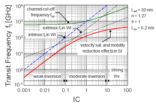
Characterization and Modeling of nanoscale MOSFET for RF designSubthreshold Operation for Ultra Low-Power RF CircuitsIn the same way power is traded against speed in subthreshold digital circuits, operating frequency can be traded with power consumption by shifting the bias points of RF MOSFETs from strong inversion into weak inversion. Many wireless applications are in the GHz frequency range and therefore do not need 400 GHz peak $latex f_t$ . The RF transistors’ $latex f_t$ can then be reduced by shifting their bias point from strong inversion towards weak inversion. This was already proposed by C. Enz in [25] for older technologies and lower operating frequencies. Reducing the bias current below the weak to strong inversion limit (called the specific current), while maintaining the $latex f_t$ in several tens of GHz for operation at a few GHz becomes possible with nanoscale MOSFETs. This is illustrated in Figure 1 which presents the estimated transit frequency in GHz versus the normalized bias current (represented by the inversion coefficient IC ) for a typical 65 nm CMOS low-power process.
Figure 1. Estimated trasnistion frequency vs. inversion factor
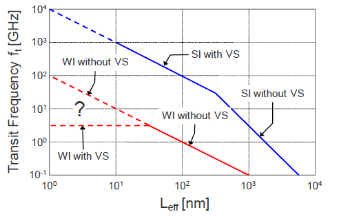
Most of the recent work in exploiting nanoscale CMOS for RF has been targeting applications in the mm-wave frequencies of typically 60 GHz and above. This requires the devices to be biased in strong inversion in order to get the maximum transit frequency close to the peak transit frequency. At such high gate and drain bias voltages, the carrier velocity is saturated. This results in a transconductance which becomes independent of the gate length and hence a transit frequency that scales as $latex 1/L_g$ instead of $latex 1/L^2_g$ when carrier velocity saturation is not present. The estimation in Figure 1 assumes that the carrier verlocity does not saturate. In a long-channel device biased in weak inversion, the carriers (electrons for an n-channel device) injected from the source diffuse towards the drain producing the drain current. In a short-channel device, the longitudinal field is no more uniform along the channel due to draininduced barrier lowering (DIBL) and the carrier injected at the source may drift towards the drain. If the channel is made small enough and the drain voltage is sufficiently high, the carrier velocity may reach the saturation velocity, in the same way it does in strong inversion. A simple calculation assuming that the carriers injected from the source are in velocity saturation in the whole channel indicates that the minimum channel length for this to occur is in the range of a few tens of nm. This means that the claimed advantage of $latex 1/L^2_g$ scaling of $latex f_t$ in weak inversion, taking full advantage of channel length reduction, would be lost also in weak inversion as it is already in strong inversion due to velocity saturation! The above argument is true when considering only the intrinsic portion of the device, neglecting the extrinsic part. $latex f_t$ is actually defined as the ratio of the gate transconductance $latex G_m$ to the total capacitance seen at the gate $latex C_G$ which is the sum of the intrinsic gate capacitance $latex C_{Gi}$ and the extrinsic gate capacitance $latex C_{Ge}$. Each of these capacitances scales differently: $latex C_{Gi}$ is proportional to the total gate oxide capacitance $latex W_g.L_g.C_{ox}$ , whereas $latex C_{Ge}$ is proportional to the gate width $latex W_g$, but does not scale with the transistor length $latex L_g$. On the other hand, the gate transconductance $latex G_m$ is proportional to the $latex W_g/L_g$ ratio as long as velocity saturation is not present, and becomes independent of $latex L_g$ in the presence of velocity saturation. From these scaling properties of $latex G_m$ and $latex C_G$ we see that $latex f_t$ can scale as $latex 1/L^2_g$, $latex 1/L_g$ or not scale at all, depending on the bias point and whether velocity saturation is present or not. In weak inversion, the total gate capacitance is dominated by the extrinsic part $latex C_{Ge}$, so that it does not scale with $latex 1/L_g$ . If velocity saturation is not present, then $latex G_m$ is proportional to $latex W_g/L_g$ and hence $latex f_t$ scales as $latex 1/L_g$ in weak inversion. This $latex 1/L_g$ scaling is similar to what happens in strong inversion in the presence of velocity saturation. As explained above, if the channel length is sufficiently small and/or the drain voltage sufficiently large, velocity saturation may also occur in weak inversion. In this case the gate transconductance $latex G_m$ becomes independent of $latex L_g$ and the transit frequency $latex f_t$ (in weak inversion) also becomes independent of $latex L_g$ and hence does not scale anymore with $latex L_g$! In other words, the advantage of $latex 1/L^2_g$ scaling initially stated for the intrinsic device in weak inversion would totally breaks down if velocity saturation would occur!
Figure 2. Transit frequency scaling with effective channel length
|
Share |